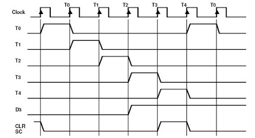
I was studying Instruction cycle from "Computer System Architecture" by Morris Mano .Under timing and control topic,fetching cycle is explained like this:
T0: AR<--PC
T1:IR<--M[AR],PC<--PC+1

IR-Instruction Register
AR-Address Register
PC-Program Counter
However, according to my understanding of previous topics PC can be incremented with T0 control signal.Please explain is it possible?/

Recommended Answers

All 6 Replies

First of all, I'm not familiar to that particular book you mention, so I don't really know what you mean by T0 and T1. I can tell you however thet the code you wrote down indeed is a fetch cycle. Your program counter tells you on which line in your assembler program (or whatever you call your higher level language) you are. So first of all, you want to fetch that line from memory to your IR in order to decode and execute it. When that's done, and your micro code is finished, you want to restart your fetch cycle, but with the next line in your assembler memory. Right?

Also, you only want to increment your PC once. The logical to do this is in the second line (T1). This is because you are already reading/writing from your PC during the first line. If you would increment the PC simultaneously as you are reading from it, you never know wether you get PC or PC+1, right? So in order to avoid problems, it's better to increment it after you've read from it.

I hope I managed to answer your question. If not, please specify your question a little more.

Good luck to you!
Emil Olofsson

T0 and T1 are control signals or we can say a clock cycles.
You have given an appropriate answer as I was also thinking the same.But what driving me in confusion is this explaination that I've read in the book--:
"The two microoperations DR<--AC and AC<--DR can be executed at the same clock cycle.This can be done by placing the content of AC on the bus,enabling load input of DR,transfering th content of the adder and logic circuit into AC and enabling the load input of AC,all during the same clock cycle.The two tranfers occur at the end of the clock cycle."
Now,how can this mutual transfer be possible as the data in both registers is changing?/
Please refer these images Bus system and Timing.

Well, from what I manage to extract from this is that DR<--AC goes the traditional way via the bus. However, When you say AC<--DR it looks like you tell your arithmetic logic unit (ALU) to perform the task AC<--DR, letting AC just fall right through the ALU ending up at DR. I see what you mean as DR is both put on the bus and loaded at the same time (it seems). This is all about timing and is somewhat machine-specific. My guess is that when the data from AC reaches DR, the previous contents of DR are already making its way through the ALU. On your machine this may be possible, however, in order to avoid unpleasant surprises I try to avoid reading/writing at the same time unless I've got access to a datasheet that explains exactly what happens on which clock-flank.

so we can conclude that read/write can be done at same time but it's hardware specific and is generally avoided.

Well, yeah. If you don't know enough about the specific system you are working with I suggest you should avoid reading and writing to the same register at the same time. You'll never know what will happen, unless you've got access to a datasheet that tells you exactly what happens to all regiterss at every clock-flank.

Please mark this thread as solved if you are satisfyed by my answers!

Regards,
Emil Olofsson

I was confused because I missed that arithmetic circuit in the figure also gets the control/timing signals and it's not continuously putting data into AC.Now it's clear.

Thanks a lot

Be a part of the DaniWeb community

We're a friendly, industry-focused community of developers, IT pros, digital marketers, and technology enthusiasts meeting, networking, learning, and sharing knowledge.