Intel revealed a new fiber-optic interface yesterday, capable of transferring an entire HD movie in a single second. Curious, considering they've yet to release their relatively modern Light Peak technology that transfers data at an already astounding 10Gbit/sec. Their new interface ups the ante five-fold, and opens the door for even greater speeds down the road.
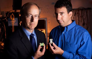
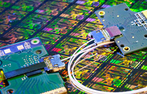
The so-far nameless interface is powered by an integrated hybrid laser (indium phosphide) inside the controller chip. Light Peak is based on an external laser and this reorganizing of components provides Intel with the boost in transmission rates. They refer to the integrated design as “silicon photonics”. In order to achieve 50Gbit/sec, data is encoded across four laser beams of varying wavelengths, at 12.5Gbit/sec. According to Mario Paniccia (an Intel fellow ), “50Gbits/sec is just the beginning.”
Gizmodo's Sam Biddle breaks down the physics behind silicon photonics, and why we may need it sooner than we think:
The fundamental process is that of transferring data by converting electrons—which are what make the device you're reading this on right now work—into photons. Intel's photonic technology uses a dazzling bit of engineering—and I do mean dazzling, as we're on the scale of your fingernail—to encode data into laser streams. These streams converge into one, and travel along a fiber-optic strand to their destination, where they are decoded from light back into electrons.
Why would we need anything as complicated and sophisticated as this? The fact of the matter is that we're nearing the limit of what we can do with electrons—and there's no arguing with physics. Once we get in the realm of 10 gigabit transfer speeds, we've pushed copper wiring about as far as it will go without degrading the signal beyond usefulness. And with the mind boggling volume of data swirling around—HD movies, lossless audio, high resolution photos—what might sound excessive today will be essential sooner than we think. Intel's announcement has to do with their research, rather than a specific product, such as Light Peak. Paniccia reassures us that Light Peak is still relevant in the short term. In regards to their new tech, he says,“This is not a technology that’s ten years away, but maybe three to five years. Light Peak, as we’ve stated, will launch next year.” They still have to optimize the transmission rates and numbers of beams used to carry data, but they hope to reach speeds of 1Tbit/sec when the product eventually hits the market.
Intel (and consumers) hope they can keep the cost of their optical interfaces low by continuing to develop the integrated lasers and using existing chip manufacturing techniques. By limiting the number of separate components, it will probably be cheaper that the less powerful Light Peak. In regards to cost and the silicon photonics, Paniccia says, “We have a passive connector without any fancy stages, so we believe we’ve discovered a low-cost, high-volume assembly.” He also has high hopes that Light Peak and their integrated interface will do away with the need for different cables for each task, “...with low-cost optics, in the future everything can be connected by fiber. We can revolutionize the way data moves about.”
[ Intel ]