Intel crams GPU into new "Sandy Bridge" CPUs

PCBrown 0 Tallied Votes 493 Views Share

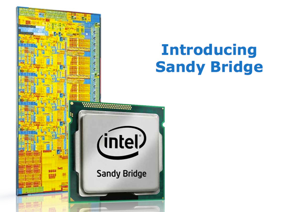
Intel’s latest line of processors, code named “Sandy Bridge”, was designed with intense multimedia demands in mind. Although we won’t likely see a sandy bridge chip on the market until early 2011, we have learned a good deal of information in regards to the architecture of the processor.

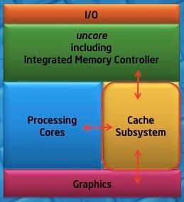
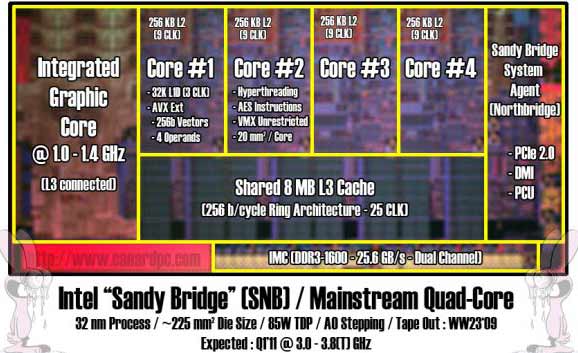
The greatest leap in design is the debut of silicon that is devoted to transcoding data. Think data conversion. An everyday example would be the transcoding of audio and video data when playing a media file that requires a special codec (QuickTime, DivX, i.e.) for playback or converting something between two formats, be it for your iPod, or PSP, for example. The current “Nehalem” processor lineup is wonderful, but having dedicated CPU power for playing media should create a notable difference in the overall, modern PC user-experience. Intel has also crammed a GPU into the Sandy Bridge, another first for the company. It will sit on the same silicon wafer as the main processor, no small feat in and of itself, through the advent of the miniscule 32 nanometer transistor manufacturing process. The smaller measurement brings cooler temps and greater space efficiency to the design table. The GPU and transcoding functions will be backed by new processor instructions for handling media, dubbed Advanced Vector Extension, or Intel AVX for short.

Even though the Core i3, i5, and i7 processors cut the mustard, consumer interest in upgrading PCs has leveled out. This is the perfect time for a dramatic shift in CPU design and Intel’s CEO Paul Otellini recognizes the opportunity at hand, as heard during a conference call last month. "Due to the very strong reception of Sandy Bridge, we have accelerated our 32-nanometer factory ramp...to enable us to meet the anticipated demand”.


[ CNET ]
Dani AI

Generated

Good summary from . A few practical, build-focused details worth adding for anyone reading this thread later:

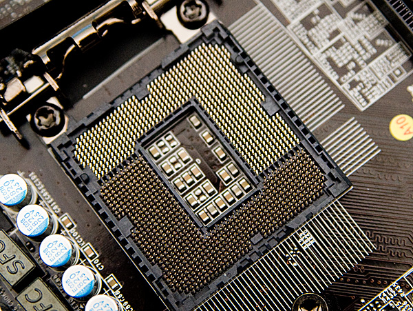
Sandy Bridge desktop parts used the LGA1155 socket, so an older LGA1156 board is not compatible. Two mainstream chipset paths mattered at launch: H67 (routes the CPU’s on-die video to the board I/O, so the integrated graphics/video engine can be used) and P67 (aimed at discrete-GPU and overclocking builds, with BIOS options for multiplier tuning). Intel’s unlocked "K" SKUs were the enthusiast choice for multiplier overclocking.

Intel’s hardware video engine (marketed as Quick Sync) made common H.264 encode/decode workloads much faster and lighter on the CPU. Early application support was uneven, so adoption improved as drivers and encoders were updated. HTPC-style builds often favored an H67 board plus the on-chip video for a quiet, power-efficient media system.

For gaming or serious GPU work, the common route was a P67 board with a discrete GPU and a K-series CPU; many P67 boards also offered beefier VRMs and BIOS controls. Across the board, BIOS and chipset-driver updates were important for stability and compatibility, especially on early boards and firmware.

A final note: initial platform revisions had a few errata that required vendor BIOS updates and later silicon revisions, so checking board revision and firmware history was recommended when evaluating older Sandy Bridge hardware. Thanks to for the original overview and to for the short follow-up that reflects the launch buzz.

dhanushkasampat 0 Newbie Poster

sandy bridge

Be a part of the DaniWeb community

We're a friendly, industry-focused community of developers, IT pros, digital marketers, and technology enthusiasts meeting, networking, learning, and sharing knowledge.