
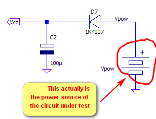
I recently built a logic probe adapting a circuit from an old magazine. One of the modifications I introduced is adding a polarity protection diode (1N4007) in series with the positive power rail, because the probe is intended to be powered from the circuit under test and I want to avoid damaging the probe should I mistakenly connect the power rails to the wrong place.
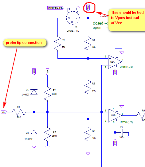
This has led to a small error in the definition of the voltage levels the probe recognizes as HIGH and LOW. That's because the thresholds are defined by a 3-resistors divider placed across the rails, which in the original design sensed the actual supply voltage of the circuit under test, and which now suffers from a 0.7V drop due to the protection diode.
I didn't want to modify heavily the circuit, so I thought of connecting the upper leg of the divider directly to the power rail of the circuit under test, bypassing the protection diode. I simulated the circuit with LTspice and everything is fine.
Here are the schematics for the input stage and the power supply stage:
My question is: is this design decision risky in case of a polarity inversion in the rails?
In this case I reckon that the current that may flow along "wrong paths" will be heavily limited by the resistors of the divider, which are rather large. Moreover the divider is connected to the inputs of an LM358 opamp, which should be quite insensitive to reverse voltages spikes of modest energy content (it's a bipolar design, so no MOSFET gates that can be damaged by voltage spikes even if current-limited).
Am I missing something? Is my reasoning correct?
P.S.: I assume a max reverse voltage of 20V (worse scenarios are less likely, and I won't bother to design a foolproof protection scheme for those).
